


CVD Graphene Film Specifications
| Growth Method | CVD Synthesis |
|---|---|
| Quality Control | Raman, SEM, and Optical |
| Transparency | ~97.7% |
| Graphene Thickness (Å) | 3.45 |
| Cu Grain Orientation | Predominantly Cu(111) |
| Cu Catalyst Thickness (µm) | 20 |
| Average Crystal Size (catalyst) | cm-scale |
| Average Graphene Grain Size (µm) | ~80 |
| Multilayer Coverage (%) | < 5% |
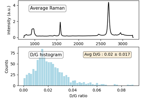
| I2D/IG Average - after transfer | > 1.6 |
| ID/IG Average - after transfer | < 0.05 |
| 2D peak FWHM (cm-1) - after transfer | ~ 35 |
| Sheet Resistance (Ω/sq) - on SiO2/Si wafer | 500 +/- 70 ohms/sq |
| Mobility (cm2/Vs)* (dep on transfer) | > 3000 |
| Appearance | Transparent film |
| PMMA Thickness | 280 nm |
| PMMA Molecular Weight | 950 kDa |
Applications
Biosensors, membranes, heating films, fundamental research.
Product Documentation
References

Clay Wright
Presbyterian College
★★★★★
"General Graphene provides large quantities of high-quality graphene at a low cost that I have used in my research studying electrodeposition on 2D materials. In addition, they have gone above and beyond to address specific requests for my own research."

Kohei Matsuda
Filgen, Inc.
★★★★★
"We have handled CVD graphene from various suppliers as an importer, but General Graphene's CVD graphene is definitely differentiated by its large grain size and competitive price. Its quality is also supported by the fact that many of our customers order it repeatedly."

Sara Abouelniaj
Graphene Grids
★★★★★
"As a growing startup, having a dependable graphene supplier is critical—and General Graphene has exceeded expectations. Their deep materials expertise, responsive team, and fast turnaround times have made them an invaluable partner in keeping our operations smooth and efficient."

Henk Postma
Younicity Inc.
★★★★★
"General Graphene has been and continues to be instrumental during the R&D phase of our project, and their expertise in graphene deposition has been invaluable. They listened carefully to our requirements in sample handling and tailored their approach to meet our specific needs. Their collaborative spirit and technical depth have accelerated our development process."

Srivatsa Aithal
Director of R&D, Hememics Biotechnologies
★★★★★
"We have worked with GG's team for years now and have primarily used large crystal and polycrystalline graphene. GG has provided us with excellent customer service, technical support, and consistent quality. We value their reliability and innovation."

Mike Musgnug
CEO, GrapheneDx
★★★★★
"GG’s expertise in scalable graphene materials manufacturing, combined with their collaborative scientific support, enabled our team to rapidly develop and iterate sensors for advanced medical diagnostics. Their professionalism and responsiveness exceeded our expectations."

Prof. Piran Kidambi
Vanderbilt University
★★★★★
"General Graphene's consistent quality of monolayer CVD graphene and large production capacity stands out. We've successfully used their material in multiple research projects, enabling progress we couldn't achieve with other suppliers."

Alok Kumar, Ph.D.
MGH, Harvard Medical School
★★★★★
"GG's graphene foam is an exceptional substrate material for cell culture. We observed improved cell growth and differentiation, making their products an integral part of our biomaterials research."

Eric Kriegstein
CEO, Infusense
★★★★★
"General Graphene is a world-class engineering organization. We successfully worked with the group to develop and prototype components for electrochemical sensing applications, and their attention to detail, commitment to solving technical challenges, and technical prowess is second to none."

Dr. Deji Akinwande
Chair Professor, University of Texas at Austin
★★★★★
General Graphene has provided us with high-quality graphene samples, which we have used to advance our research in flexible electronics and sensor devices. Their professionalism and reliability are unmatched in the industry."

Dr. Daniel Molin
Maastricht University
★★★★★
General Graphene has provided us with high-quality graphene samples, which we have used to advance our research in flexible electronics and sensor devices. Their professionalism and reliability are unmatched in the industry."